|
|
|
Finite element analysis of temperature distribution of polycrystalline silicon thin film transistors under self-heating stress |
Huaisheng WANG, Mingxiang WANG( ), Zhenyu YANG ), Zhenyu YANG |
| Department of Microelectronics, Soochow University, Suzhou 215021, China |
|
|
|
|
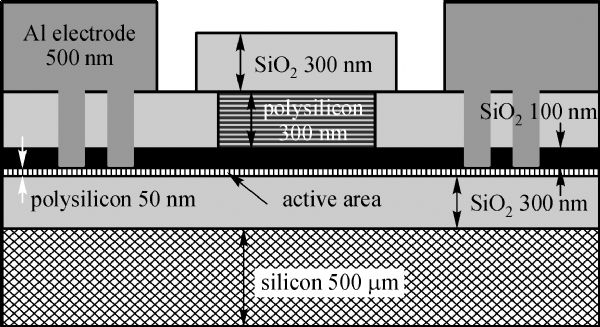
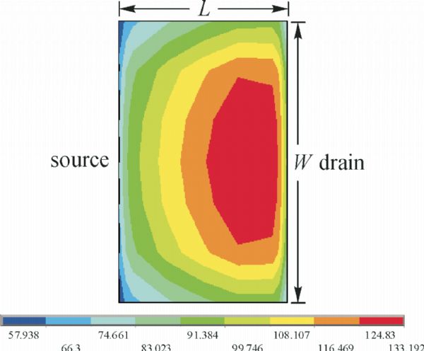
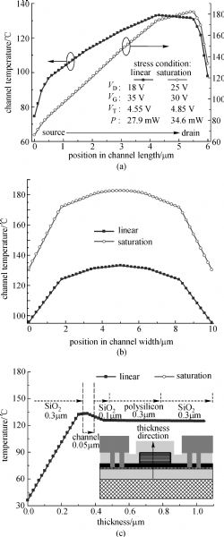
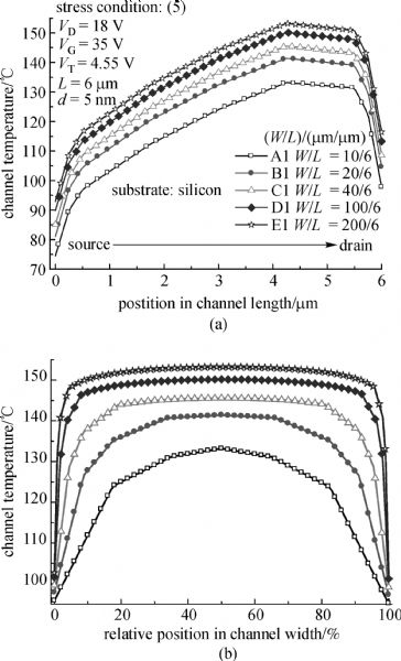
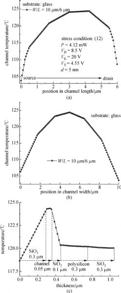
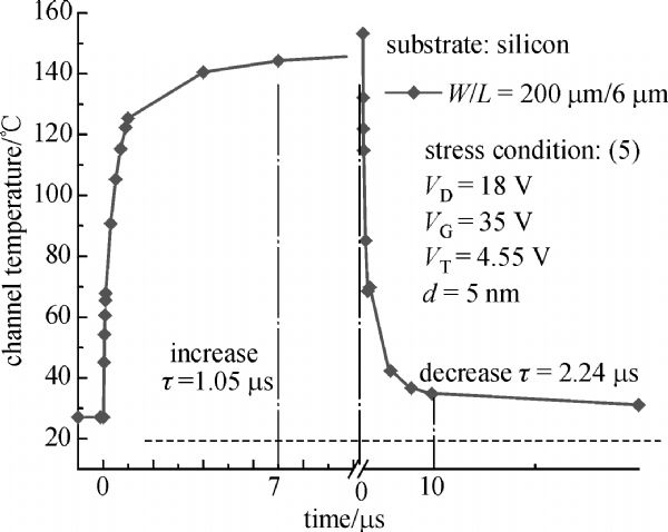
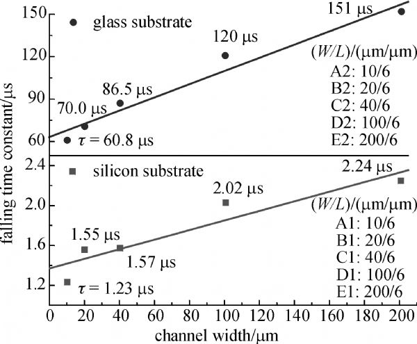
Abstract The temperature distribution of typical n-type polycrystalline silicon thin film transistors under self-heating (SH) stress is studied by finite element analysis. From both steady-state and transient thermal simulation, the influence of device power density, substrate material, and channel width on device temperature distribution is analyzed. This study is helpful to understand the mechanism of SH degradation, and to effectively alleviate the SH effect in device operation.
|
| Keywords
finite element analysis (FEA)
temperature distribution
thin film transistors
self-heating
steady-state
transient state
|
|
Corresponding Author(s):
WANG Mingxiang,Email:Mingxiang_wang@suda.edu.cn
|
|
Issue Date: 05 June 2009
|
|
| 1 |
Wang W, Meng Z G, Guo H C. High performance metal-induced unilaterally crystallized polycrystalline silicon thin-film transistors: technology and applications. Chinese Journal of Liquid Crystals and Displays , 2002, 17(5): 323–330 (in Chinese).
|
| 2 |
Inoue S, Ohshima H, Shimoda T. Analysis of degradation phenomenon caused by self-heating in low-temperature-processed polycrystalline silicon thin film transistors. Japanese Journal of Applied Physics , 2002, 41(11): 6313–6319
doi: 10.1143/JJAP.41.6313
|
| 3 |
Fuyuki T, Kitajima K, Yano H, Hatayama T, Uraoka Y, Hashimoto S, Morita Y. Thermal degradation of low temperature poly-Si TFT. Thin Solid Films , 2005, 487(1-2): 216–220
doi: 10.1016/j.tsf.2005.01.068
|
| 4 |
Wang H S, Wang M X, Yang Z Y, Hao H, Wong M. Stress power dependent self-heating degradation of metal induced laterally crystallized n-type polycrystalline silicon thin film transistors. IEEE Transactions on Electron Devices , 2007, 54(12): 3276–3284
doi: 10.1109/TED.2007.908907
|
| 5 |
Jomaah J, Ghibaudo G, Balestra F. Analysis and modeling of self-heating effects in thin-film SOI MOSFETs as a function of temperature. Solid-State Eleclronics , 1995, 38(3): 615–618
doi: 10.1016/0038-1101(94)00130-8
|
| 6 |
Sameshima T, Sunaga Y, Kohno A. Measurements of temperature distribution in polycrystalline thin film transistors caused by self-heating. Japanese Journal of Applied Physics , 1996, 35(3A): 308–310
doi: 10.1143/JJAP.35.L308
|
| 7 |
Cahill D G, Ford W K, Goodson K E, Mahan G D, Majumdar A, Maris H J, Merlin R, Phillpot S R. Nanoscale thermal transport. Journal of Applied Physics , 2003, 93(2): 793–818
doi: 10.1063/1.1524305
|
| 8 |
McConnell A D, Uma S, Goodson K E. Thermal conductivity of doped polysilicon Layers. Journal of Microelectromechanical Systems , 2001, 10(3): 360–369
doi: 10.1109/84.946782
|
| 9 |
Glassbrenner C J, Slack G A. Thermal conductivity of silicon and germanium from 3 K to the melting point. Physical Review , 1964, 134(4A): A1058–A1069
doi: 10.1103/PhysRev.134.A1058
|
| 10 |
Cahill D G. Thermal conductivity measurement from 30 to 750 K: the 3ωmethod. Review of Scientific Instruments , 1990, 61(2): 802–808
doi: 10.1063/1.1141498
|
| 11 |
Corning Incorporated. Corning 1737 AMLCD Glass Substrates Material Information. 2004, MIE 101
|
| 12 |
Sze S M, Kwok K NG. Physics of Semiconductor Devices. 3rd ed. American: John Wiley & Sons, 2007, 303–306
|
| 13 |
Tummala R R. Fundamentals of Microsystems Packaging. American: McGraw-Hill Companies, 2001, Chapter 6.4
|
|
Viewed |
|
|
|
Full text
|
|
|
|
|
Abstract
|
|
|
|
|
Cited |
|
|
|
|
| |
Shared |
|
|
|
|
| |
Discussed |
|
|
|
|