|
|
|
Preparation and optimization of freestanding GaN using low-temperature GaN layer |
Yuan TIAN1,2,3, Yongliang SHAO1( ), Xiaopeng HAO1, Yongzhong WU1, Lei ZHANG1, Yuanbin DAI1, Qin HUO1, Baoguo ZHANG1, Haixiao HU1 ), Xiaopeng HAO1, Yongzhong WU1, Lei ZHANG1, Yuanbin DAI1, Qin HUO1, Baoguo ZHANG1, Haixiao HU1 |
1. State Key Lab of Crystal Materials, Shandong University, Jinan 250100, China
2. Key Lab of Advanced Transducers and Intelligent Control System (Ministry of Education), Taiyuan University of Technology, Taiyuan 030024, China
3. College of Physics and Optoelectronics, Taiyuan University of Technology, Taiyuan 030024, China |
|
|
|
|
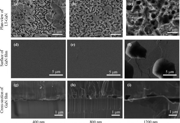
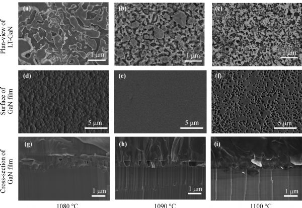
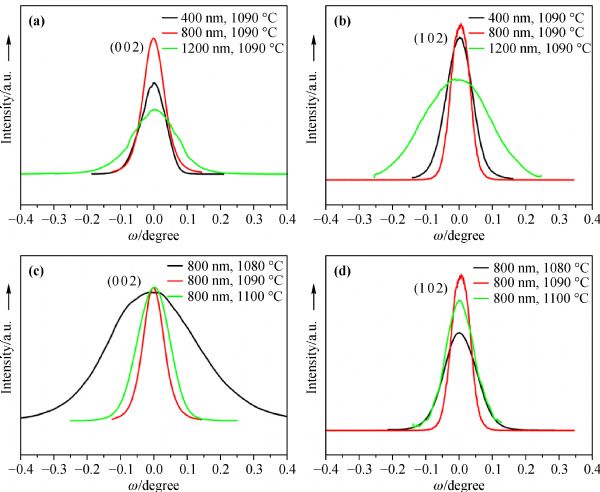
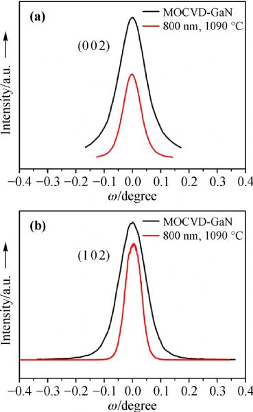
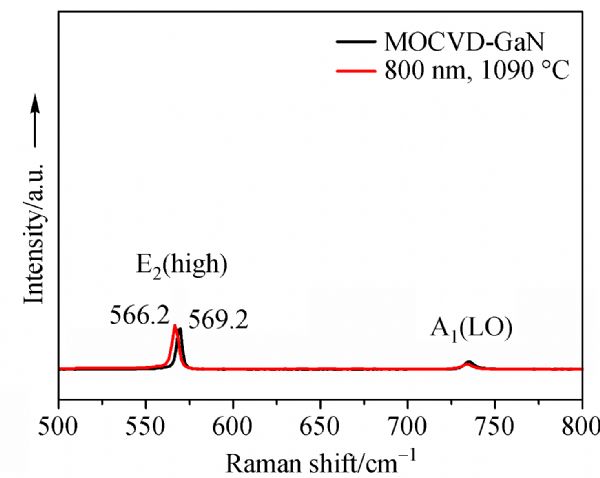
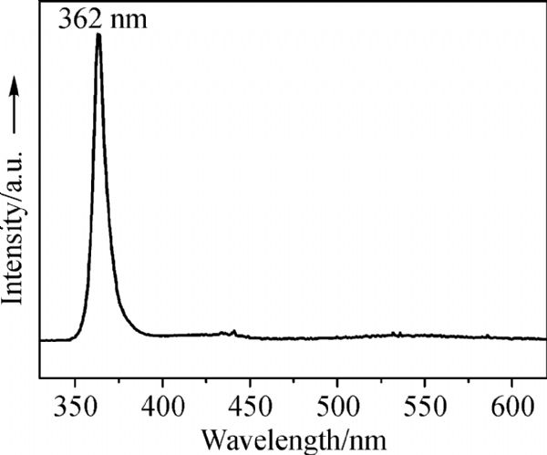
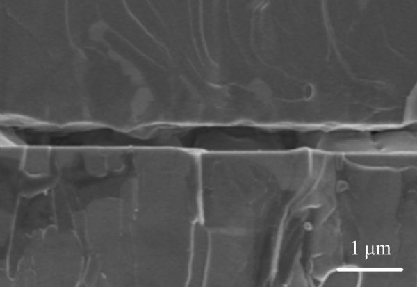
Abstract In this work, a method to acquire freestanding GaN by using low temperature (LT)-GaN layer was put forward. To obtain porous structure and increase the crystallinity, LT-GaN layers were annealed at high temperature. The morphology of LT-GaN layers with different thickness and annealing temperature before and after annealing was analyzed. Comparison of GaN films using different LT-GaN layers was made to acquire optimal LT-GaN process. According to HRXRD and Raman results, GaN grown on 800 nm LT-GaN layer which was annealed at 1090 °C has good crystal quality and small stress. The GaN film was successfully separated from the substrate after cooling down. The self-separation mechanism of this method was discussed. Cross-sectional EBSD mapping measurements were carried out to investigate the effect of LT-buffer layer on improvement of crystal quality and stress relief. The optical property of the obtained freestanding GaN film was also determined by PL measurement.
|
| Keywords
GaN
self-separation
low-temperature
annealing
|
|
Corresponding Author(s):
Yongliang SHAO
|
|
Online First Date: 03 July 2019
Issue Date: 29 September 2019
|
|
| 1 |
V Darakchieva, T Paskova, P P Paskov, et al.. Residual strain in HVPE GaN free-standing and re-grown homoepitaxial layers. Physica Status Solidi A: Applied Research, 2003, 195(3): 516–522
https://doi.org/10.1002/pssa.200306145
|
| 2 |
E Richter, M Gründer, B Schineller, et al.. GaN boules grown by high rate HVPE. Physica Status Solidi C: Current Topics in Solid State Physics, 2011, 8(5): 1450–1454
https://doi.org/10.1002/pssc.201000901
|
| 3 |
W Luo, X Wang, H Xiao, et al.. Growth and fabrication of AlGaN/GaN HEMT based on Si (111) substrates by MOCVD. Microelectronics Journal, 2008, 39(9): 1108–1111
https://doi.org/10.1016/j.mejo.2008.01.083
|
| 4 |
Y Cui, L Li. Evolution of spirals during molecular beam epitaxy of GaN on 6H-SiC (0001). Physical Review B: Condensed Matter, 2002, 66(15): 155330
https://doi.org/10.1103/PhysRevB.66.155330
|
| 5 |
S I Cho, K Chang, M S Kwon. Strain analysis of a GaN epilayer grown on a c-plane sapphire substrate with different growth times. Journal of Materials Science, 2007, 42(10): 3569–3572
https://doi.org/10.1007/s10853-007-1562-5
|
| 6 |
W Qian, M Skowronski, M De Graef, et al.. Microstructural characterization of α-GaN films grown on sapphire by organometallic vapor phase epitaxy. Applied Physics Letters, 1995, 66(10): 1252–1254
https://doi.org/10.1063/1.113253
|
| 7 |
H M Kim, J E Oh, T W Kang. Preparation of large area free-standing GaN substrates by HVPE using mechanical polishing liftoff method. Materials Letters, 2001, 47(4‒5): 276–280
https://doi.org/10.1016/S0167-577X(00)00249-4
|
| 8 |
M K Kelly, R P Vaudo, V M Phanse, et al.. Large free-standing GaN substrates by hydride vapor phase epitaxy and laser-induced liftoff. Japanese Journal of Applied Physics, 1999, 38(Part 2, No. 3A): L217–L219
https://doi.org/10.1143/JJAP.38.L217
|
| 9 |
Y Oshima, T Eri, M Shibata, et al.. Fabrication of freestanding GaN wafers by hydride vapor-phase epitaxy with void-assisted separation. Physica Status Solidi, 2002, 194(2): 554–558
https://doi.org/10.1002/1521-396X(200212)194:2<554::AID-PSSA554>3.0.CO;2-B
|
| 10 |
Y Oshima, T Eri, M Shibata, et al.. Preparation of freestanding GaN wafers by hydride vapor phase epitaxy with void-assisted separation. Japanese Journal of Applied Physics, 2003, 42(Part 2, No.1A/B): L1–L3
https://doi.org/10.1143/JJAP.42.L1
|
| 11 |
C L Chao, C H Chiu, Y J Lee, et al.. Freestanding high quality GaN substrate by associated GaN nanorods self-separated hydride vapor-phase epitaxy. Applied Physics Letters, 2009, 95(5): 051905
https://doi.org/10.1063/1.3195684
|
| 12 |
K Motoki, T Okahisa, S Nakahata, et al.. Preparation of large GaN substrates. Materials Science and Engineering B, 2002, 93(1‒3): 123–130
https://doi.org/10.1016/S0921-5107(02)00048-X
|
| 13 |
L Zhang, Y Shao, X Hao, et al.. Improvement of crystal quality HVPE grown GaN on an H3PO4 etched template. CrystEngComm, 2011, 13(15): 5001–5004
https://doi.org/10.1039/c1ce05147d
|
| 14 |
L Zhang, Y Dai, Y Wu, et al.. Epitaxial growth of a self-separated GaN crystal by using a novel high temperature annealing porous template. CrystEngComm, 2014, 16(38): 9063–9068
https://doi.org/10.1039/C4CE01188K
|
| 15 |
D Gogova, A Kasic, H Larsson, et al.. Strain-free bulk-like GaN grown by hydride-vapor-phase-epitaxy on two-step epitaxial lateral overgrown GaN template. Journal of Applied Physics, 2004, 96(1): 799–806
https://doi.org/10.1063/1.1753073
|
| 16 |
B Gibart, P Beaumont, P Vennegues. Nitride semiconductors. In: P Ruterana, M Albrecht, J Neugebauer, eds. Handbook on Materials and Devices. Weinheim, Germany: Wiley-VCH, 2003, 45
|
| 17 |
Y Tian, Y Shao, Y Wu, et al.. Direct growth of freestanding GaN on C-face SiC by HVPE. Scientific Reports, 2015, 5(1): 10748
https://doi.org/10.1038/srep10748
pmid: 26034939
|
| 18 |
S Tripathy, S J Chua, P Chen, et al.. Micro-Raman investigation of strain in GaN and AlxGa1−xN/GaN heterostructures grown on Si(111). Journal of Applied Physics, 2002, 92(7): 3503–3510
https://doi.org/10.1063/1.1502921
|
| 19 |
C Kisielowski, J Krüger, S Ruvimov, et al.. Strain-related phenomena in GaN thin films. Physical Review B: Condensed Matter, 1996, 54(24): 17745–17753
https://doi.org/10.1103/PhysRevB.54.17745
pmid: 9985904
|
| 20 |
P Boguslawski, E L Briggs, J Bernholc. Native defects in gallium nitride. Physical Review B, 1995, 51(23): 17255–17258
https://doi.org/10.1103/PhysRevB.51.17255
pmid: 9978750
|
| 21 |
F J Xu, B Shen, L Lu, et al.. Different origins of the yellow luminescence in as-grown high-resistance GaN and unintentional-doped GaN films. Journal of Applied Physics, 2010, 107(2): 023528
https://doi.org/10.1063/1.3294965
|
| 22 |
J L Lyons, A Janotti, C G Van de Walle. Carbon impurities and the yellow luminescence in GaN. Applied Physics Letters, 2010, 97(15): 152108
https://doi.org/10.1063/1.3492841
|
| 23 |
O Ambacher, M S Brandt, R Dimitrov, et al.. Thermal stability and desorption of Group III nitrides prepared by metal organic chemical vapor deposition. Journal of Vacuum Science & Technology B, 1996, 14(6): 3532–3542
https://doi.org/10.1116/1.588793
|
| 24 |
A Rebey, T Boufaden, B El Jani. In situ optical monitoring of the decomposition of GaN thin films. Journal of Crystal Growth, 1999, 203(1‒2): 12–17
https://doi.org/10.1016/S0022-0248(99)00081-0
|
| 25 |
B V L’vov. Kinetics and mechanism of thermal decomposition of GaN. Thermochimica Acta, 2000, 360(1): 85–91
https://doi.org/10.1016/S0040-6031(00)00558-X
|
| 26 |
Y Shao, L Zhang, X Hao, et al.. Large area stress distribution in crystalline materials calculated from lattice deformation identified by electron backscatter diffraction. Scientific Reports, 2014, 4: 5934 (5 pages)
https://doi.org/10.1038/srep05934
pmid: 25091314
|
| 27 |
Y Shao, Y Dai, X Hao, et al.. EBSD crystallographic orientation research on strain distribution in hydride vapor phase epitaxy GaN grown on patterned substrate. CrystEngComm, 2013, 15(39): 7965–7969
https://doi.org/10.1039/c3ce40802g
|
| 28 |
A J Wilkinson, P B Hirsh. Electron diffraction based techniques in scanning electron microscopy of bulk materials. Micron, 1997, 28: 279–308
|
| 29 |
N Stanford, D Dunne, M Ferry. Deformation and annealing of (011)[011] oriented Al single crystals. Acta Materialia, 2003, 51(3): 665–676
https://doi.org/10.1016/S1359-6454(02)00445-7
|
|
Viewed |
|
|
|
Full text
|
|
|
|
|
Abstract
|
|
|
|
|
Cited |
|
|
|
|
| |
Shared |
|
|
|
|
| |
Discussed |
|
|
|
|